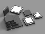
Three Things to Know About QFN Packages
Posted by Admin on 30th Aug 2021
The QFN (Quad Flat No-lead) package is a popular semiconductor package. It is gaining popularity in the electrical market because of its low cost, small form factor, and its reliable thermal performance. These miniature packages are used widely in various consumer, industrial, automotive, and power applications. In PCBs, this leadless package offers moderate heat dissipation. Flat no-lead packages include a central thermal pad for improving the heat transfer on the circuit board. The heat transferring holes in the thermal pad is drilled in a matrix format for preventing the displacement of the component during soldering that could lead to poor thermal functionalities.
In the QFN fabrication and assembly process, soldering plays an important role. It is used for joining the various electrical connections together. Several problems can arise during soldering, such as voiding in QFNs. Such voiding can occur when volatiles become entrapped underneath the pad upon reflow. The soldering process must be confirmed carefully to avoid shorts, voids, opens, and deficiencies that can cause manufacturing and reliability concerns. You can customize and buy QFN stencil and control its aperture size and other factors to better release the volume of solder paste on the PCB. The modifications in aperture reduction, aperture design, thickness, and pad design can help to improve the efficiency and quality of the soldering process.
QFN Assembly
In the surface-mounting of components in the QFN assembly process, one needs to follow the given basic steps. Primarily, you need to apply solder paste on the board before placing the components. As per the layout which you decide during the PCB design stage, you need to place the QFN IC components on the board. Perform pre-reflow inspection to ensure that the board is appropriately prepared to go into the reflow oven. It helps in removing the surrounding contaminants. You can solder the QFN components using reflow soldering and then subject them to quality inspection again.
Types Of QFN Packages
As per the molding method, there are two types of QFN packages, namely, punch-type and sawn-type. Punch-type packages are molded in a single mold cavity format. Sawn-type packages are molded using the mold array process (MAP). The large package set is cut into parts in this method.
What Are The Advantages Of QFN Packages?
QFN packages have small footprints and a thin package. It is lightweight and easy to handle. It comes in a thin profile and has a small form factor. It has excellent thermal performance, and the board provides a path for heat transfer from die to the board. Because of its small form factor, the various parts can be placed closer to other components on the board. The lead inductance of QFN packages is low. It is ideal for applications that need good heat dissipation capabilities. Moreover, with this package, there are no lead co-planarity issues. The contact pads of QFN packages are exposed and it is flushed with the package bottom.
To Conclude:
These are a few important basics regarding QFN packages. It helps in connecting the IC silicon die to the circuit board and provides moderate heat dissipation in PCBs. Understanding the basics will help you to improve the quality and accuracy of the QFN assembly process.

